Low-Noise Global Shutter Pixels for CMOS Image Sensors
The image quality of CMOS image sensors has been greatly improved as high as that of CCD image sensors.
However, the high image quality provided by CMOS image sensors is restricted to rolling shutter operation.
In global shutter imaging, CMOS image sensors have poor image quality due to kTC noise(reset noise).
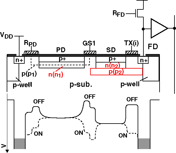
A developed two-stage charge transfer pixel enables kTC noise canceling by means of true correlated double sampling. An implemented prototype has demonstrated for the first time that a noise level of less than 3 electrons can be achieved in a global-shutter CMOS image sensor while attaining a high shutter efficiency of 99.7%.
The CMOS image sensor has been presented at ISSCC 2010.
 |
 |
| Fig.1 Proposed two-stage charge transfer pixel |
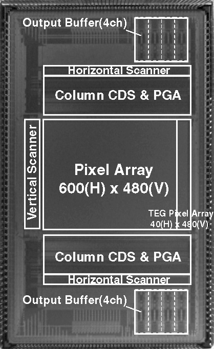
Fig.2 The developed CMOS imager |
 |
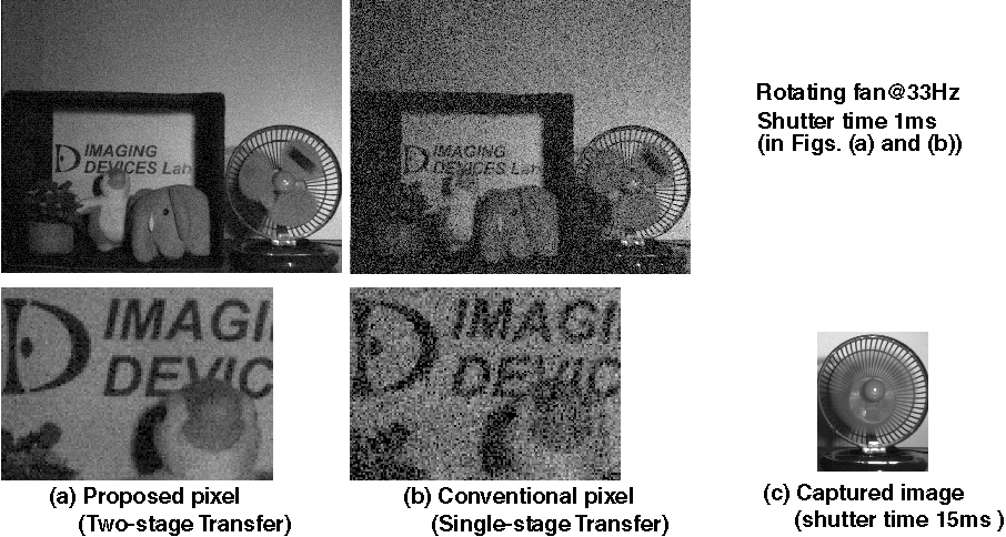
| Fig.3 Captured images with the developed imager for comparison between the proposed and conventional structure.
|
Refernces
- K. Yasutomi, Y. Sadanaga, T. Takasawa, S. Itoh, S. Kawahito,"Dark Current Characterization of CMOS Global Shutter Pixels using Pinned Storage Diodes," Proc. 2011 Int. Image Sensor Workshop(IISW), pp.185-188, Hakodate, Jun. 2011.
- K. Yasutomi, S. Itoh, S. Kawahito,"A Two-Stage Charge Transfer Active Pixel CMOS Image Sensor with Low-Noise Global Shuttering and a Dual Shuttering Mode," IEEE Trans. Electron Devices, Vol.58, No.3, pp.740-747, Mar.2011.
- K. Yasutomi, S. Itoh, S. Kawahito,"A 2.7e- temporal noise 99.7% shutter efficiency 92dB dynamic range CMOS image sensor with dual global shutter pixels," IEEE Int. Solid-State Circuits Conf.(ISSCC) 2010, Dig. Tech. Papers, pp398-399, San Francisco, Feb.2010
- K. Yasutomi, S. Itoh, S. Kawahito, T. Tamura,"Two-stage charge transfer pixel using pinned diodes for low-noise global shutter imaging," Int. Image Sensor Workshop, pp.333-336, Bergen, Jun.2009
- K. Yasutomi, T. Tamura, M. Furuta, S. Itoh, S. Kawahito," A high-speed CMOS image sensor with global electronic shutter pixels using pinned diode," IEEJ Trans. on Sensors and Micromachines, vol.129, no.10, pp.321-327,Oct.2009.
[Home] / [Research project]
Copyright(C)1999-2010, Imaging Devices Laboratory
e-mail: [email protected]
